Physics of Semiconductors
The metal/organic
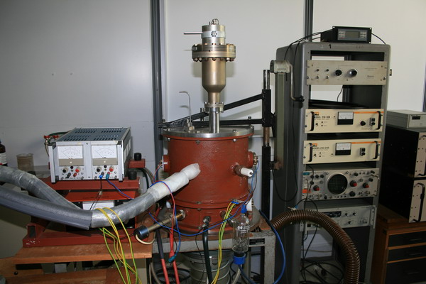
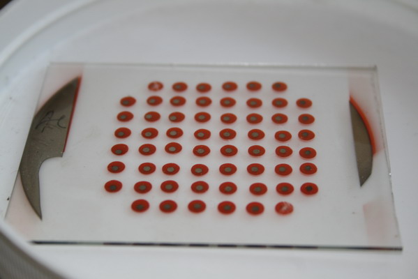
semiconductor/metal structures as deposited by the ionized
cluster beam vacuum deposition method may under suitable
conditions serve as simple radiation sensors. For this
purpose the physical processes related to the current
through such a structure should be well understood, but it
is the fact that some basic characteristics still remain to
be clarified even nowadays. Thus for instance it was only
recently that the research associates have been able to show
that the conjecture of the (coupled) drift-diffusion
electron transport interpreted in terms of the model of
shallow traps occupying a single energy level is
incompatible with the published measurements.
For some decades
it is being generally accepted that the electric current
through the metal/organic semiconductor contact is modeled
under the assumption of vanishing electric field at the
junction. This assumption results in an infinity charge
carrier density at the charge-injecting (metal) electrode,
which however is being commonly interpreted as the
occurrence of the space charge limited current effect, SCLC,
in strong analogy with the exceedingly high electron density
surrounding the cathode in vacuum tubes of the past.
Postulating the
non-zero electric field at such an interface, the associates
have recently shown, considering the model of traps
exponentially distributed in energy within the organic
semiconductor charge transport band, that the interfacial
and the external electric field are coupled via the
non-linear algebraic equation the solutions of which (at
each bias) result in the spatial distribution of the
electron density (and of the internal electric field) that
is within the organic and at its boundaries everywhere
finite and continuous. In addition, it was shown that when
the interfacial field is directly proportional to the
externally applied electric field the resulting current
follows the power law of the external bias resulting (in
contrast to the generally accepted notion) in the negligible
SCLC effect. However, the latter may indeed become
significant if the non-zero interfacial field remains
constant (i.e. bias independent) in which case the electric
current turns out to be a concave function of bias. It is
argued that the combination of the interfacial electric
field linearly dependent upon the applied bias up to a given
value of the external electric field and constant thereafter
results in the current density, which exhibits distinct line
slopes in the current- voltage plane.
The
described novelties were tested on a number of published
measurements and a good agreement with the experiments has
been obtained.
1. M. Koželj, B. Cvikl, D. Korošak: Properties
of organic Schottky junctions under the influence of
ionizing radiation. Proceedings of the 42th International
Conference on Microelectronics, Devices and Materials and
the Workshop on MEMS and NEMS, p. 77-82, September, 13. -
15, 2006, Strunjan, Slovenia.
2. B. Cvikl. On an example of the space charge
limited conduction breakdown in relation to the
current-voltage characteristics of a single layer
metal/organic structure. J. Appl. Phys., 104, p. 113721-(7)
(2008).
3. B. Cvikl. The drift-diffusion interpretation of the
electron current within the organic semiconductor
characterized by the bulk single energy trap level. J. Appl.
Phys., 107, p. 023710-(9), (2010).
4. B. Cvikl. The elimination of interface
charge density singularity in single layer organic
semiconductor structures. J. Appl. Phys., 110, p.
033723-(9), (2011).
5. M. Koželj, B. Cvikl. Comments on the
current-voltage interpretation of organic diodes by the
model of traps exponentially distributed in energy.
Proceedings of the 48th International Conference on
Microelectronics, Devices and Materials and the Workshop on
Ceramic Microsystems, p. 163-167, September, 19. -
21, 2012, Otočec, Slovenia.
6. CVIKL, Bruno. Current-voltage line
shapes of single layer metal/organic semiconductor
structures as response to the electric field at the charge
injecting interface. Thin Solid Films, (2012), submitted.
